

Semiconductor manufacturing relies on specialised components to maintain precision and quality. These components enable critical processes inside sealed environments.
One essential element allows visual monitoring while keeping chambers perfectly sealed. This dual function supports both observation and energy transmission needs.
Various stainless steel and glass materials meet different operational requirements. The right material choice ensures durability and optimal performance.
This how-to guide explores the practical applications of these components. We’ll examine their role across different semiconductor manufacturing stages.
Proper selection directly impacts process efficiency and final product quality. Understanding these applications helps optimise manufacturing outcomes.
Key Takeaways
- Specialised viewports maintain seal integrity while enabling visual access
- They serve dual purposes: process observation and energy transmission
- Material selection varies by specific semiconductor application needs
- Proper component choice affects manufacturing efficiency and yield quality
- Different manufacturing stages require specific viewport characteristics
- Stainless steel and high-quality glass are common construction materials
- Understanding applications helps optimise semiconductor production processes
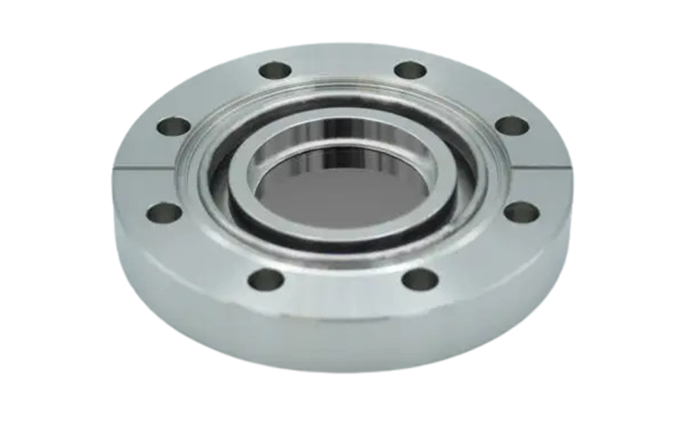
Understanding Vacuum Viewports and Their Role in Semiconductor Tools
Observation components provide crucial visibility into otherwise inaccessible manufacturing processes.
These specialised optical windows maintain complete environmental isolation. They use advanced hermetic sealing techniques to preserve chamber integrity.
Three primary functions define the purpose of vacuum viewports in semiconductor equipment. First, they enable visual monitoring of internal processes. Second, they allow illumination of the chamber interior. Third, they transmit various energy forms to affect processes.
Various semiconductor manufacturing tools utilise these components. Etching systems, deposition equipment, and implantation tools all require visual access points. Each application has specific material and design requirements.
| Chamber Size Range | Typical Applications | Viewport Requirements |
| 10-50 cm | Research & Development | Small diameter, basic sealing |
| 50-200 cm | Pilot Production | Medium size, enhanced durability |
| 200+ cm | Full-scale Manufacturing | Large format, premium materials |
| Specialty (e.g., 122 ft) | Research Facilities | Custom engineering, extreme specifications |
Semiconductor processes operate under different pressure conditions. High vacuum environments typically range from 10⁻³ to 10⁻⁷ torr. Ultra-high vacuum systems reach pressures below 10⁻⁹ torr.
Laser applications represent another critical use case. Optical monitoring systems rely on clear transmission paths. Energy delivery for process modification requires precise optical components.
Outgassing rates significantly impact semiconductor manufacturing quality. Low-outgassing materials prevent contamination of sensitive processes. Proper material selection ensures minimal particulate generation.
Real-world examples include plasma etching observation and deposition rate monitoring. These applications demonstrate the practical importance of visual access components. Process engineers rely on them for quality control and troubleshooting.
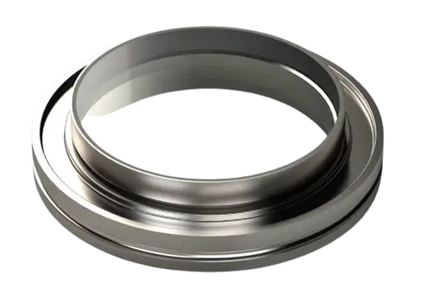
Material choices vary by specific application needs. Glass options provide excellent optical clarity. Metallic alternatives offer enhanced durability for demanding environments.
Selecting the Right Viewport Material for Semiconductor Applications
Material selection forms the foundation of optical component performance in semiconductor tools. The correct choice ensures both visual clarity and chamber integrity throughout manufacturing processes.
Different materials offer unique advantages for specific applications. Understanding these properties helps optimise semiconductor production outcomes.
| Material Type | Transmission Range | Max Bake Temperature | Primary Applications |
| Borosilicate Glass | Visible spectrum | 200°C | General observation, plasma monitoring |
| Fused Silica (Quartz) | UV to DUV | 200°C | Laser systems, precision optics |
| Sapphire | UV to NIR | 450°C | High-temperature processes |
| Zinc Selenide | Infrared | 150°C | Thermal imaging, IR applications |
| Magnesium Fluoride | VUV to mid-IR | 250°C | Broad spectrum applications |
| Calcium Fluoride | VUV to IR | 300°C | Laser-resistant environments |
Borosilicate glass provides excellent visible light transmission with minimal distortion. Its thermal shock resistance makes it suitable for various semiconductor environments.
Fused silica, also known as quartz, offers outstanding UV transmission capabilities. This material type excels in precision optics and laser applications.
Sapphire delivers remarkable durability across extreme conditions. Its broad transmission range covers ultraviolet to near-infrared spectra.
Infrared applications often benefit from zinc selenide components. This material provides high IR transmission for thermal monitoring systems.
Magnesium fluoride covers an exceptionally wide spectral range. From vacuum ultraviolet to mid-infrared, it maintains consistent performance.
Calcium fluoride offers the broadest transmission capabilities among common materials. It combines chemical resistance with laser damage tolerance.
Thermal properties significantly influence material selection. Maximum bake temperatures determine suitability for high-temperature processes.
Chemical resistance proves crucial in aggressive semiconductor environments. Process gases and cleaning agents can degrade incompatible materials.
Mechanical durability varies considerably between material types. Scratch resistance affects long-term performance and maintenance requirements.
Cost-performance tradeoffs require careful consideration. Premium materials like sapphire justify investment in critical applications.
Laser applications demand specific optical characteristics. Precision requirements include minimal absorption and scatter properties.
Environmental factors guide final material selection. Temperature fluctuations, pressure conditions, and chemical exposure all influence choices.
Real-world examples demonstrate practical material applications. Lithography systems typically use fused silica for its DUV transmission.
Etching chambers often employ borosilicate glass for plasma observation. Deposition tools may require sapphire for high-temperature visibility.
Proper material selection directly impacts manufacturing efficiency. The right choice reduces downtime and improves process control.
Quality considerations include outgassing rates and particulate generation. Low-contamination materials preserve sensitive semiconductor processes.
Custom coatings can enhance base material performance. Anti-reflective treatments improve transmission for specific wavelength ranges.
Application-specific requirements should drive material decisions. Matching material properties to process needs ensures optimal results.
- Evaluate transmission needs across UV, visible, and IR spectra
- Consider thermal requirements including bake temperatures
- Assess chemical compatibility with process environments
- Balance mechanical durability against cost constraints
- Factor in precision needs for laser and optical systems
- Review environmental conditions and exposure risks
Material science continues advancing semiconductor capabilities. New compositions offer improved performance for emerging applications.
Key Specifications for Semiconductor Vacuum Viewports
Technical specifications directly determine the operational capabilities of optical access components. These detailed requirements ensure reliable performance across diverse semiconductor manufacturing environments.
Bakeout temperature specifications vary significantly by material and construction. Standard CF/KF flange configurations typically handle 150°C, while O-rings extend this range to 250°C. Quartz materials withstand 200°C, and sapphire components tolerate extreme temperatures up to 450°C.
Thermal gradient limitations prevent stress fractures during temperature changes. Standard components handle 25°C per minute, while specialty materials require slower 20°C per minute rates. Premium products need careful 3°C per minute ramping.
Transmission performance spans multiple wavelength ranges with different efficiency levels. Broadband anti-reflection coatings on quartz achieve remarkable 99% efficiency in specific spectral bands.
These coating options include both single-layer and multi-layer BBAR configurations. Each coating type optimises performance for particular wavelength applications. Proper coating selection maximizes energy transmission while minimizing reflection losses.
Flange material choices include 304 stainless steel for general applications. More demanding environments may require 316LN stainless steel or titanium options. Each material offers distinct advantages for specific operational conditions.
Outgassing rate specifications prove critical for ultra-high vacuum semiconductor applications. Low outgassing materials prevent contamination of sensitive manufacturing processes. This specification directly impacts final product quality and yield rates.
Size and dimensional requirements vary by chamber configuration and application needs. Standard sizes accommodate most production equipment, while custom dimensions serve specialised research facilities. Proper sizing ensures optimal integration with existing systems.
Pressure rating specifications relate directly to material choices and construction quality. Higher ratings typically require premium materials and enhanced sealing technologies. These ratings ensure safety and reliability under operational conditions.
Quality control standards follow stringent UHV manufacturing protocols. Cleaning procedures eliminate particulate contamination that could affect semiconductor processes. ISO 9001:2015 certification ensures consistent quality across production batches.
These comprehensive specifications form the foundation for component selection. Understanding each parameter helps optimise semiconductor manufacturing outcomes. Proper specification matching ensures long-term reliability and process consistency.
Implementing Vacuum Viewports in Specific Semiconductor Processes
Semiconductor fabrication demands precise component integration across diverse manufacturing stages. Each process requires tailored optical access solutions to maintain quality and efficiency.
Lithography systems benefit from fused silica components. These materials provide exceptional deep ultraviolet transmission for pattern transfer accuracy.
Etching chambers present challenging corrosive environments. Sapphire and calcium fluoride materials withstand aggressive chemical exposure while maintaining visibility.
These robust options prevent clouding and degradation during plasma etching operations. Their chemical resistance ensures consistent performance over extended periods.
Deposition systems operate at elevated temperatures. High-temperature viewports maintain seal integrity while allowing process observation.
Thermal processing applications require specific transmission characteristics. Infrared-compatible materials enable accurate temperature monitoring and control.
Metrology systems demand exceptional optical clarity. Precision transmission ensures accurate measurement and inspection results.
Laser processing applications need specialised components. Calcium fluoride offers excellent laser damage resistance for trimming operations.
Cleanroom installation requires meticulous contamination control. Proper handling procedures prevent particulate introduction during component integration.
Integration with pumping systems needs careful planning. Pressure monitoring equipment connects seamlessly with properly specified viewports.
Coating selection varies by specific application needs. Anti-reflective treatments optimise performance for particular wavelength ranges.
Single-layer coatings suit specific laser wavelengths. Broadband options cover wider spectral ranges for multi-purpose applications.
These implementation considerations ensure optimal performance across different semiconductor processes. Proper selection directly impacts manufacturing yield and quality.
Real-world success stories demonstrate practical implementation benefits. One foundry improved yield by 3% through optimised viewport selection.
Another manufacturer reduced downtime by implementing sapphire viewports in etching tools. Their enhanced durability withstood aggressive cleaning cycles.
Advanced coating technologies continue evolving to meet new challenges. Emerging applications demand increasingly sophisticated optical solutions.
Proper implementation follows established best practices while allowing customisation. Each semiconductor process has unique requirements that guide final selection.
Installation and Maintenance Best Practices
Proper handling ensures optical components function correctly in semiconductor tools. Following guidelines prevents damage and maintains chamber integrity.
Installation begins with careful unpacking. Always wear clean gloves to protect surfaces. Inspect components for shipping damage before proceeding.
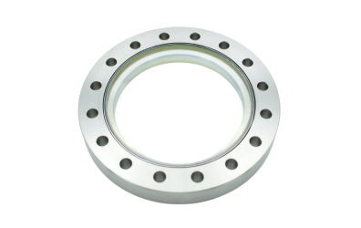
Different flange types require specific installation approaches. Each connection style has unique sealing characteristics and torque requirements.
| Flange Type | Torque Specification | Seal Material | Temperature Limit |
| CF (ConFlat) | 120-140 in-lbs | Copper gasket | 450°C |
| KF (Quick Flange) | 60-80 in-lbs | Viton O-ring | 200°C |
| ISO | 90-110 in-lbs | Kalrez O-ring | 250°C |
| Custom Flanges | Per manufacturer | Various options | Varies |
Cleaning follows strict UHV protocols. Use only approved solvents and lint-free wipes. Avoid touching optical surfaces during cleaning.
Maintenance schedules depend on operational intensity. High-use systems need monthly inspections. Low-use applications may require quarterly checks.
O-ring replacement follows specific guidelines. Some of these rings are suitable for high-temperature applications up to 250°C. Always use manufacturer-specified replacement parts.
Bakeout procedures require careful temperature control. The maximum heating rate should not exceed 3°C per minute. This prevents thermal stress damage.
Leak detection uses helium mass spectrometry. Regular testing ensures chamber integrity. Document all test results for quality records.
Safety protocols protect both personnel and equipment. Always depressurise systems before maintenance. Use proper lifting equipment for heavy components.
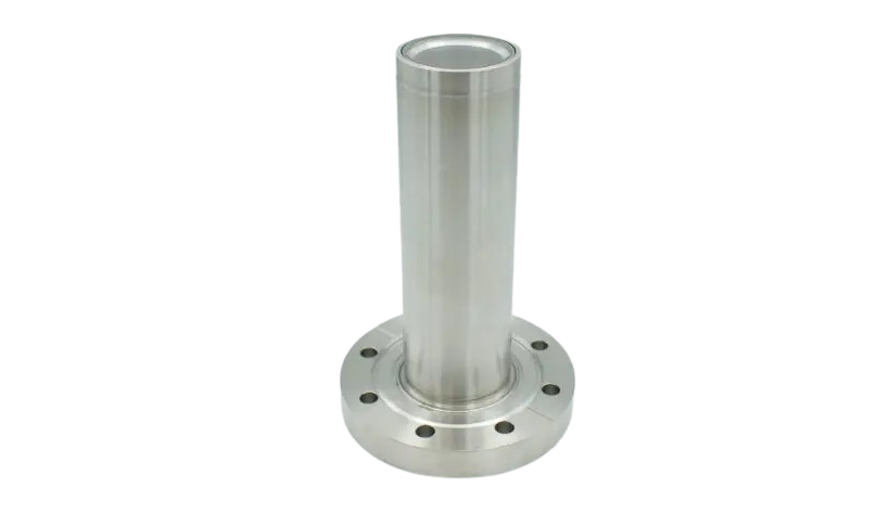
Demountable designs allow substrate removal for cleaning. This feature simplifies maintenance without breaking seals. It also enables custom coating upgrades.
Recessed zero-profile designs offer maximum protection. They provide wide viewing angles while shielding optical surfaces. This design reduces contamination risks.
Quality control teams verify every product before shipment. They ensure compliance with semiconductor industry standards. This includes cleanliness and performance testing.
Documentation maintains compliance with quality systems. Keep detailed records of all maintenance activities. Include installation dates, inspections, and replacements.
Troubleshooting common issues requires systematic approach. Most problems relate to improper installation or damaged seals. Follow manufacturer guidelines for resolution.
Proper installation and maintenance extend component lifespan. They also ensure consistent manufacturing quality. Following best practices reduces downtime and costs.
Optimising Your Semiconductor Vacuum Viewport Selection
Intelligent component selection directly influences semiconductor manufacturing outcomes and yield rates. The right choices balance performance requirements with economic considerations across different production scales.
Material optimisation involves careful analysis of transmission needs and environmental conditions. Custom coatings enhance performance for specific wavelength ranges while reducing reflection losses.
Future-proofing requires considering evolving technology demands and scalability needs. Partnering with experienced suppliers ensures access to professional advice and custom solutions.
Total cost analysis should include maintenance requirements and long-term reliability factors. Performance benchmarking against industry standards helps validate selection decisions for critical semiconductor applications.